Overcoming Design Challenges: Tips for Effective PCB Routing and Placement
September 26, 2023Designing a printed circuit board (PCB) can be a complex and time-consuming task, especially when routing and placing components on it. As technology advances, PCBs become more intricate with increasingly smaller components that require careful placement to ensure efficient performance.
To make the design process easier and more effective, this article outlines key tips for successful PCB routing and placement. From selecting the right materials to understanding signal integrity requirements, readers will gain valuable insight into how to overcome common design challenges while creating optimal solutions for their projects.
Utilizing Available Tools to Reduce Design Complexity
When it comes to PCB routing and placement, utilizing the right tools can make a huge difference in reducing design complexity. By having access to powerful software packages that offer automated schematic capture capabilities, designers can quickly create complex designs without the time-consuming task of manually routing components.
Additionally, with the use of advanced simulation and optimization tools, engineers can better assess their design decisions and ensure that they are meeting all required parameters for their application. Finally, having an accurate Bill of Materials (BOM) is essential for any project’s success; modern BOM management systems allow teams to easily check component availability and pricing while ensuring accuracy throughout production. With these types of available tools at hand, designers will be well-equipped to reduce design complexity as much as possible when working on PCB routing and placement projects.
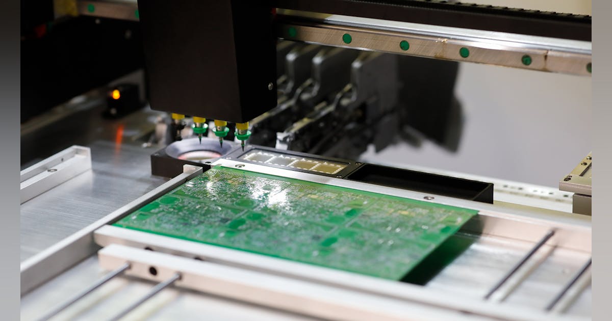
Analyzing the Impact of Component Placement on Signal Integrity

Source: resources.pcb.cadence.com
When designing a printed circuit board (PCB), component placement is an important factor to consider when it comes to achieving signal integrity. Poorly placed components can lead to undesirable electrical characteristics, such as crosstalk and signal reflections which can affect the quality of data being transmitted across the board.
As such, designers must be aware of the implications of improper component placement on PCBs to optimize performance and avoid costly errors during production. Designers must take into account several factors when considering the impact of component placement on signal integrity including impedance matching, trace length control, and electromagnetic interference (EMI) shielding requirements. Impedance matching involves selecting components with appropriate impedances that match those found in other parts throughout the system; this helps ensure consistent power delivery between different sections of a PCB layout.
Trace length control refers to keeping traces as short as possible while avoiding sharp turns or excessive bends; this reduces reflections caused by mismatched impedances along trace lengths and improves overall signal integrity. Lastly, EMI shielding requires certain components to be placed near each other so they are adequately shielded from noise generated by adjacent circuits; these shields must also not interfere with any signals that need to pass between them for optimal performance across a PCB layout.
By understanding how component placement affects signal integrity, designers will be able to reduce design complexity while improving product functionality and reliability for their customers’ systems.
Understanding How Different PCB Materials Affect Routing and Placement
When designing a printed circuit board (PCB), there are many factors to consider, including the type of material used. Different PCB materials can have a dramatic effect on routing and placement, so it is important to understand which materials will best suit your design needs.
The most common types of PCB material include FR4, polyimide, liquid crystal polymer (LCP), and ceramic substrate boards. Each has its advantages and disadvantages when it comes to routing and placement.
For example, FR4 is often chosen for its low cost but may not be suitable for complex layouts due to limited thermal resistance or signal integrity issues. Polyimide offers superior flexibility and excellent heat dissipation properties making it an ideal choice for high-density designs requiring small components in tight spaces; however, these benefits come with higher costs associated with production processes such as lamination.
LCP boards offer improved signal integrity along with good solderability but require specialized tools during assembly due to their fragile nature while ceramic substrates provide better thermal performance than FR4 but require additional care during handling because they are more prone to cracking or shattering under pressure. Ultimately choosing the right PCB material should depend on the complexity of your design requirements and budget constraints – understanding how different materials affect routing and placement is key to getting the most out of your PCB design project!
Using Automatic Routing Strategies to Improve Efficiency
Source: electronicdesign.com
Automatic routing strategies are an invaluable tool for streamlining the process of PCB routing and placement. By leveraging advanced algorithms, designers can create highly efficient designs with fewer resources than ever before.
With these automated tools, engineers can quickly and accurately determine optimal routes for signal traces on a board while also ensuring that components are placed in the most effective positions. Designers can even optimize their designs to reduce manufacturing costs by taking advantage of shorter trace paths.
By utilizing automatic routing strategies, engineers can dramatically improve their efficiency and save time on design projects without sacrificing quality or accuracy.
Conclusion
Designing PCBs can be a challenging task, but with the right knowledge and techniques, it doesn’t have to be. By understanding the basics of PCB routing and placement, designers can create high-performance circuits that meet their desired specifications without compromising on quality.
With proper planning and organization, designers can identify potential challenges before they occur and adjust accordingly for maximum efficiency. The key is to make sure that all components are correctly placed to ensure good signal integrity as well as power management while keeping noise levels low.
Taking these steps will lead to the successful completion of the design project, ensuring satisfaction among clients with an effective PCB routing and placement solution.